Definition:
The forward current developed by the A10 charging switch exceeded 175 AMPs or the "ON" drive remained on in excess of 275 micro-seconds.
Theory:
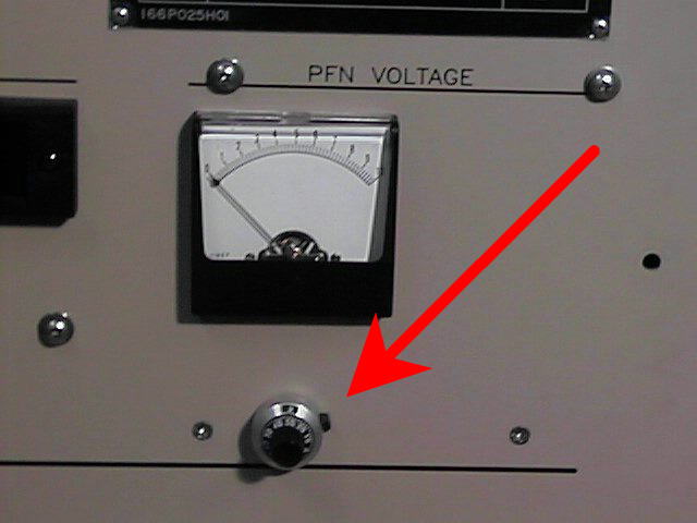
The A10 "Charging Switch" (figure 11-5, sheet 2) supplies current ( 175 Amps max ) to the charging transformer (A7T2) producing a magnetic field. When the "charging switch" turns off, the magnetic field collapses. The longer the switch is on, the greater the energy stored in the "charging transformer" will be. The "on" time must not exceed 275 micro-seconds. The collapsing field induces a charge into the PFN through the A12A5 diode assembly. The collapsing field develops a ring or flyback that is shunted by the "flyback diodes".
Additional charging switch information:
The A10 "Charging Switch" turns on internal transistors upon reception
of "MODCHRGTR-" (modulator charge trigger) if the proper enabling signals
are true (28VDC from A2K1D, HVONRMPRTN and CHGEN). The length of
time that the transistors are on is controlled by comparing the current
sample from A10T4 (top right of figure 11-5, sheet2) and a voltage sample
(top left of figure 11-5, sheet 2) from A1R3
on
signal PFNWDREF for wide pulse and A1A2R74 on
signal PFNNARREF for narrow pulse. Selection of reference signal
is determined by the signal PFNSHAPER which is a indication of the PFN's
switch position.
A10 "Charging Switch" Wave forms
Sampling Point(s):
The forward current is sampled in the A10, "charging switch" by T4.
Top, right of figure 11-5, sheet 2
The time limit is checked by the driving circuits on the A10A1
board. Top, center of figure 11-5, sheet 2
Detection/Threshold Point(s):
The sample is monitored by the circuits in the A10A1 card inside the
charging switch. See figure11-5 sheet 2, left of center.
Supporting Indications:
The "TIME-OUT FAULT LED" (left of center on figure 11-5, sheet3) should be illuminated when this fault is present. Remember the fault is no longer detected after a fault reset.
Wave forms measured at A10A1 TP1 and TP2 ( OFF and ON drive) show a on time near 275 micro-seconds.
Comparison of the wave form at TP7 could be compared to a wave form made earlier (baseline measurments) to determine if there is a substantial change in current. This would only be of value if your system was measured in good operating condition with a known PFN voltage and no modulator components had been replaced.
Conflicting Indications:
Supporting Documentation:
EHB 6-511
Last Updated on October 02, 1998